Black silicon: engineering an intermediate band in silicon for photovoltaic applications,
at
240th National Meeting of the American Chemical Society (Boston, MA),
Wednesday, August 25, 2010:
Optical hyperdoping: black silicon
Pushing a physics discovery towards commercial impact,
at
APS March meeting (Boston, MA),
Thursday, March 1, 2012:
Laser-processing of semiconductors for solar energy harvesting applications,
at
Laser World of Photonics conference (Mumbai, India),
Tuesday, November 12, 2013:
Non-equilibrium materials by fs-laser texturing and hyperdoping of silicon,
at
AFOSR Ultrashort Pulse Laser-Matter Interactions PI Review (Arlington, VA),
Thursday, June 2, 2016:
Silicon microtexturing using ultrashort laser pulses,
at
MRSEC Site visit, Harvard University (Cambridge, MA),
Saturday, February 17, 2001:
Femtosecond laser-assisted microstructuring of silicon for novel detector, sensing, and display technologies,
at
State Key Laboratory for Silicon Material Lecture, Zhejiang University (Hangzhou, China),
Thursday, October 17, 2002:
Optoelectronic devices using femtosecond laser microstructured silicon,
at
NATO ASI Course on New developments in optics and related fields: modern techniques, materials, and applications, Centro Ettore Majorana (Erice, Italy),
Sunday, June 12, 2005:
Femtosecond laser doping of silicon beyond the equilibrium limit,
at
Photonics West 2009 (San Jose, CA),
Tuesday, January 27, 2009:
Black silicon,
at
Institute of Physics in Ireland 2009/2010 Lecture, Trinity College (Dublin, Ireland),
Friday, March 12, 2010:
Femtosecond laser doped silicon for photovoltaic applications,
at
SPIE Optics & Photonics (San Diego),
Friday, August 12, 2011:
Mid-infrared absorptance of silicon hyperdoped with chalcogens via fs-laser irradiation,
at
Black Silicon Symposium (Albany, NY),
Thursday, August 9, 2012:
Black silicon,
at
2013 Swenton-Ouellette Lecture, Ohio State University (Columbus, OH),
Thursday, February 14, 2013:
Laser-assisted microstructuring of silicon surfaces for novel detector, sensing, and display technologies,
at
Physics and Advanced Technologies Seminar, Lawrence Livermore National Laboratory (Livermore, CA),
Tuesday, October 16, 2001:
Femtosecond laser-assisted microstructuring of silicon surfaces for novel detector, sensing, and display technologies,
at
LEOS 2003 Annual Meeting (Tucson, AZ),
Sunday, October 26, 2003:
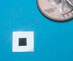 Black silicon is made by shining a series of very short, very intense laser pulses at a silicon surface in a chamber filled with sulfur-rich gas. Black silicon, in contrast, absorbs nearly all light at wavelengths ranging from the ultraviolet to the infrared. This suggests it may be very useful in improving the performance of existing silicon devices, such as detectors and photovoltaics.