Optical hyperdoping: black silicon

M. T. Winkler, M. Sher, Y. Lin, M. J. Smith, H. Zhang, S. Gradečak, and E. Mazur. 2012. “Studying femtosecond-laser hyperdoping by controlling surface morphology.” Journal of Applied Physics, 111, Pp. 093511–. Publisher's VersionAbstract
We study the fundamental properties of femtosecond-laser (fs-laser) hyperdoping by developing techniques to control the surface morphology following laser irradiation. By decoupling the formation of surface roughness from the doping process, we study the structural and electronic properties of fs-laser doped silicon. These experiments are a necessary step toward developing predictive models of the doping process. We use a single fs-laser pulse to dope silicon with sulfur, enabling quantitative secondary ion mass spectrometry, transmission electron microscopy, and Hall effect measurements. These measurements indicate that at laser fluences at or above 4 kJ m-2, a single laser pulse yields a sulfur dose > (3 ± 1) x 1013 cm–2 and results in a 45-nm thick amorphous surface layer. Based on these results, we demonstrate a method for hyperdoping large areas of silicon without producing the surface roughness.
J. E. Carey and E. Mazur. 2003. “Femtosecond Laser-Assisted Microstructuring of Silicon for Novel Detector, Sensing and Display Technologies.” In . LEOS 2003. Publisher's VersionAbstract
Arrays of sharp, conical microstructures are obtained by stucturing the surface of a silicon wafer using femtosecond laser-assisted chemical etching. The one step, maskless structuring process drastically changes the optical, material and electronic properties of the original silicon wafer. These properties make microstructured silicon viable for use in a wide range of commercial devices including solar cells, infrared photodetectors, chemical and biological sensors, and field emission devices.
T. Sarnet, J. E. Carey, and E. Mazur. 2012. “From black silicon to photovoltaic cells, using short pulse lasers.” In . International Symposium on High Power Laser Ablation 2012. Publisher's VersionAbstract
Laser created Black Silicon has been developed since 1998 at Harvard University. The unique optical and semiconducting properties of the black silicon first lead to interesting applications for sensors (photodetectors, thermal imaging cameras…). Other applications like Photovoltaic solar cells have been rapidly identified, but it took more than ten years of research and development before demonstrating a real improvement of the photovoltaic efficiency on an industrial multi-crystalline solar cell. This paper is a brief review of the use of black silicon for photovoltaic cells.
M. J. Smith, Y. Lin, M. Sher, M. T. Winkler, E. Mazur, and S. Gradecak. 2011. “Pressure-induced phase transformations during femtosecond-laser doping of silicon.” J. Appl. Phys., 110, Pp. 053524–. Publisher's VersionAbstract
Silicon hyperdoped with chalcogens via femtosecond-laser irradiation exhibits unique near-unity sub-bandgap absorptance extending into the infrared region. The intense light-matter interactions that occur during femtosecond-laser doping produce pressure waves sufficient to induce phase transformations in silicon, resulting in the formation of metastable polymorphic phases, but their exact formation mechanism and influence on the doping process are still unknown. We report direct observations of these phases, describe their formation and distribution, and consider their potential impact on sub-bandgap absorptance. Specifically, the transformation from diamond cubic Si-I to pressure-induced polymorphic crystal structures (amorphous Si, Si-XII, and Si-III) during femtosecond-laser irradiation was investigated using scanning electron microscopy, Raman spectroscopy, and transmission electron microscopy. Amorphous Si, Si-XII, and Si-III were found to form in femtosecond-laser doped silicon regardless of the presence of a gaseous or thin-film dopant precursor. The rate of pressure loading and unloading induced by femtosecond-laser irradiation kinetically limits the formation of pressure-induced phases, producing regions of amorphous Si 20 to 200 nm in size and nanocrystals of Si- XII and Si-III. The surface texturing that occurs during femtosecond-laser irradiation produces inhomogeneous pressure distributions across the surface and causes delayed development of high-pressure silicon polymorphs over many laser pulses. Finally, we find that the polymorph phases disappear during annealing more rapidly than the sub-bandgap absorptance decreases, enabling us to decouple these two processes through post-treatment annealing.
E. Landis, K. Phillips, E. Mazur, and C. M. Friend. 2012. “Formation of nanostructured TiO2 by femtosecond laser irradiation of titanium in O2.” J. Appl. Phy., 112, Pp. –. Publisher's VersionAbstract
We use femtosecond laser irradiation of titanium metal to create nanometer scale laser-induced periodic surface structures and study the influence of atmospheric composition on these surface structures. We find that gas composition and pressure affect the chemical composition of the films, but not the surface morphology. We demonstrate that irradiation of titanium in oxygen containing atmospheres forms a highly stable surface layer of nanostructured amorphous titanium dioxide.
M. Shen, J. E. Carey, C. H. Crouch, M. Kandyla, H.A. Stone, and E. Mazur. 2008. “High-density regular arrays of nanometer-scale rods formed on silicon surfaces via femtosecond laser irradiation in water.” Nano Leters, 8, Pp. 2087–2091. Publisher's VersionAbstract
We report on the formation of high-density regular arrays of nanometer-scale rods using femtosecond laser irradiation of a silicon surface immersed in water. The resulting surface exhibits both micrometer-scale and nanometer-scale structures. The micrometer-scale structure consists of spikes of 5-10 µm width, which are entirely covered by nanometer-scale rods that are roughly 50 nm wide and that protrude perpendicularly from the micrometer-scale spikes. The formation of the nanometer-scale rods involves several processes: refraction of laser light in highly excited silicon, interference of scattered and refracted light, rapid cooling in water, and capillary instabilities.
C. Wu, C. H. Crouch, L. Zhao, J. E. Carey, R. J. Younkin, J. A. Levinson, E. Mazur, R. M. Farrel, P. Gothoskar, and A. Karger. 2001. “Near-unity below-band gap absorption by microstructured silicon.” Appl. Phys. Lett., 78, Pp. 1850–1852. Publisher's VersionAbstract
We increased the absorptance of light by silicon to approximately 90% from the near ultraviolet (0.25 m) to the near infrared (2.5 m) by surface microstructuring using laser-chemical etching. The remarkable absorptance most likely comes from a high density of impurities and structural defects in the silicon lattice, enhanced by surface texturing. Microstructured avalanche photodiodes show significant enhancement of below-band gap photocurrent generation at 1.06 and 1.31 m, indicating promise for use in infrared photodetectors.
J. E. Carey. 2004. “Femtosecond-laser Microstructuring of Silicon for Novel Optoelectronic Devices”. Publisher's VersionAbstract
This dissertation comprehensively reviews the properties of femtosecond- laser microstructured silicon and reports on its first application in optoelectronic devices. Irradiation of a silicon surface with intense, short laser pulses in an atmosphere of sulfur hexafluoride leads to a dramatic change in the surface morphology and optical properties. Following irradiation, the silicon surface is covered with a quasi-ordered array of micrometer-sized, conical structures. In addition, the microstructured surface has near-unity absorptance from the near-ultraviolet (250 nm) to the near-infrared (2500 nm). This spectral range includes below-band gap wavelengths that normally pass through silicon unabsorbed. We thoroughly investigate the effect of experimental parameters on the morphology and chemical composition of microstructured silicon and propose a formation mechanism for the conical microstructures. We also investigate the effect of experimental parameters on the optical and electronic properties of microstructured silicon and speculate on the cause of below-band gap absorption. We find that sulfur incorporation into the silicon surface plays an important role in both the formation of sharp, conical microstructures and the near-unity absorptance at below-band gap wavelengths. Because of the novel optical properties, femtosecond-laser microstructured silicon has potential application in numerous optoelectronic devices. We use femtosecond-laser microstructured silicon to create silicon-based photodiodes that are one hundred times more sensitive than commercial silicon photodiodes in the visible, and five orders of magnitude more sensitive in the near-infrared. We also create femtosecond-laser microstructured silicon solar cells and field emission arrays.
A. Serpengüzel, T. Bilici, I. Inanc, A. Kurt, J. E. Carey, and E. Mazur. 2004. “Temperature dependence of photoluminescence in non-crystalline silicon.” In . Photonics West. Publisher's VersionAbstract
Crystalline silicon being ubiquitous throughout the microelectronics industry has an indirect bandgap, and therefore is incapable of light emission. However, strong room temperature visible and near-IR luminescence from non-crystalline silicon, e.g., amorphous silicon, porous silicon, and black silicon, has been observed. These silicon based materials are morphologically similar to each other, and have similar luminescence properties. We have studied the temperature dependence of the photoluminescence from these non-crystalline silicons to fully characterize and optimize these materials in the pursuit of obtaining novel optoelectronic devices.
B. R. Tull, J. E. Carey, M. A. Sheehy, C. M. Friend, and E. Mazur. 2006. “Formation of silicon nanoparticles and web-like aggregates by femtosecond laser ablation in a background gas.” Appl. Phys. A, 83, Pp. 341–346. Publisher's VersionAbstract
We show that the mechanism of nanoparticle formation during femtosecond laser ablation of silicon is affected by the presence of a background gas. Femtosecond laser ablation of silicon in a H2 or H2S background gas yields a mixture of crystalline and amorphous nanoparticles. The crystalline nanoparticles form via a thermal mechanism of nucleation and growth. The amorphous material has smaller features and forms at a higher cooling rate than the crystalline nanoparticles. The background gas also results in the suspension of plume material in the gas for extended periods, resulting in the formation (on a thin film carbon substrate) of unusual aggregated structures including nanoscale webs that span tears in the film. The presence of a background gas provides additional control of the structure and composition of the nanoparticles during short pulse laser ablation. PACS 81.16.-c
Y. Lin. 2014. “Femtosecond-laser hyperdoping and texturing of silicon for photovoltaic applications”. Publisher's VersionAbstract
This dissertation explores strategies for improving photolvoltaic efficiency and reduc- ing cost using femtosecond-laser processing methods including surface texturing and hyperdoping. Our investigations focus on two aspects: 1) texturing the silicon sur- face to create efficient light-trapping for thin silicon solar cells, and 2) understanding the mechanism of hyperdoping to control the doping profiles for fabricating efficient intermediate band materials.> We first discuss the light-trapping properties in laser-textured silicon and its benefit to thin silicon heterojunction solar cells. We report a nearly 15% improvement in the short circuit current and device efficiency after surface texturing, which is attributed to the enhancement of absorption due to the formation of Lambertian surfaces. We next present studies on the hyperdoping mechanism using a pump-probe method. We measure in situ the change in surface reflectivity during hyperdoping and extract the dynamics of the melt front. Understanding the melt dynamics allows us to constrain the physical parameters in a numerical model, which we use to simulate the doping profile with a simplified classical picture. We then demonstrate the successful fabrication of homogeneously doped silicon by manipulating the hyperdoping process based on theoretically predicted design principles.
M. Sher, Y. Lin, M. T. Winkler, E. Mazur, C. Pruner, and A. Asenbaum. 2013. “Mid-infrared absorptance of silicon hyperdoped with chalcogen via fs-laser irradiation.” J. Appl. Phys., 113, Pp. 063520–. Publisher's VersionAbstract
Silicon hyperdoped with heavy chalcogen atoms via femtosecond- laser irradiation exhibits strong broadband, sub-bandgap light absorption. Understanding the origin of this absorption could enable applications for hyperdoped-silicon based optoelectronic devices. In this work, we measure absorption to wavelengths up to 14 μm using Fourier transform infrared spectroscopy and study sulfur-, selenium- and tellurium- hyperdoped Si before and after annealing. We find that absorption in the samples extends to wavelengths as far as 6 μm. After annealing, the absorption spectrum exhibits features that are consistent with free-carrier absorption. Although the surface morphology influences the shape of the absorption curves, the data permit us to place an upper bound on the position of the chalcogen dopant energy levels.
R. J. Younkin, J. E. Carey, E. Mazur, J. A. Levinson, and C. M. Friend. 2003. “Infrared absorption by conical silicon microstructures made in a variety of background gases using femtosecond-laser pulses.” J. Appl. Phys., 93, Pp. 2626–2629. Publisher's VersionAbstract
We show that the near-unity infrared absorptance of conical microstructures fabricated by irradiating a Si(111) surface with 100-fs laser pulses depends on the ambient gas in which the structures are formed. Of the background gases we investigate, SF6 is the most effective, yielding an absorptance of 0.9 for radiation in the 1.2-2.5 m wavelength range. Use of Cl2, N2, or air produces surfaces with absorptances intermediate between that for microstructures formed in SF6 and that for flat, crystalline silicon, for which the absorptance is roughly 0.05?0.2 for a 260- m thick sample.
C. H. Crouch, J. E. Carey, M. Shen, E. Mazur, and F. Y. Genin. 2004. “Infrared absorption by sulfur-doped silicon formed by femtosecond laser irradiation.” Appl. Phys. A, 79, Pp. 1635–1641. Publisher's VersionAbstract
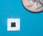
We microstructured silicon surfaces with femtosecond laser irradiation in the presence of SF6. These surfaces display strong absorption of infrared radiation at energies below the band gap of crystalline silicon. We report the dependence of this below-band gap absorption on microstructuring conditions (laser fluence, number of laser pulses, and background pressure of SF6) along with structural and chemical characterization of the material. Significant amounts of sulfur are incorporated into the silicon over a wide range of microstructuring conditions; the sulfur is embedded in a disordered nanocrystalline layer less than 1 mm thick that covers the microstructures. The most likely mechanism for the below-band gap absorption is the formation of a band of sulfur impurity states overlapping the silicon band edge, reducing the band gap from 1.1 eV to approximately 0.4 eV.
M. A. Sheehy. 2004. “Femtosecond-laser Microstructuring of Silicon: Dopants and Defects”. Publisher's VersionAbstract
This dissertation deals with the incorporation of elements into silicon using a femtosecond laser in order to understand the source for below-band gap absorptance. Previous experimental results indicate that irradiation of silicon with a femtosecond laser in the presence of sulfur hexafluoride (SF6) leads to unique optical properties. The absorptance for above-band gap radiation is increased to 95%; the more interesting result is that the below-band gap absorptance goes from nearly 0% to 90%. In the first set of experiments performed, we irradiated silicon in the presence of H2S, SiH4, and H2. The absorptance for samples prepared in H2S is identical to that of samples prepared in SF6; the other samples have a trailing edge of absorptance for energies below the band gap. This result indicated that sulfur played a crucial role in the below-band gap absorptance. The next set of experiments involved incorporating selenium and tellurium from a powder source to investigate possible dependence of the optical properties on the size of the dopant (selenium and tellurium have the same valence, but are larger in atomic size than sulfur). Incorporation of these two elements also leads to near-unity absorptance for below-band gap radiation. A comparison of the composition and the optical properties before and after annealing showed that the source for below-band gap absorptance is likely due to both the incorporated chalcogen and defects. The final set of experiments deals with the incorporation of elements from other families. These studies bolster the results of the previous research and provide furtherdetails on the interaction of the dopant with the laser- modified surface. We speculate on some requirements the dopants must satisfy (i.e. atomic size and valence onfiguration) and propose further research that can be done in this area. These experiments provide significant insight into the optical absorption mechanism and show that this material has great potential for devices that operate in the infrared portion of the spectrum, such as infrared photodiodes and solar cells.

Pages