. 2012. “Formation of nanostructured TiO2 by femtosecond laser irradiation of titanium in O2.” J. Appl. Phy., 112, Pp. –. Publisher's VersionAbstract
Optical hyperdoping: black silicon
. 2008. “High-density regular arrays of nanometer-scale rods formed on silicon surfaces via femtosecond laser irradiation in water.” Nano Leters, 8, Pp. 2087–2091. Publisher's VersionAbstract
. 2001. “Near-unity below-band gap absorption by microstructured silicon.” Appl. Phys. Lett., 78, Pp. 1850–1852. Publisher's VersionAbstract
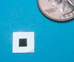 Black silicon is made by shining a series of very short, very intense laser pulses at a silicon surface in a chamber filled with sulfur-rich gas. Black silicon, in contrast, absorbs nearly all light at wavelengths ranging from the ultraviolet to the infrared. This suggests it may be very useful in improving the performance of existing silicon devices, such as detectors and photovoltaics.