Optical hyperdoping: black silicon

We have developed a novel technique that creates highly doped and structured silicon. Focusing a train of femtosecond laser pulses on silicon wafers in the presence of heavy chalcogens (e.g. S, Se, or Te) dopes a thin layer of silicon at the surface to non-equilibrium levels. This optical hyperdoping process creates black silicon, a highly absorbing surface with extended spectral sensitivity. This material offers new opportunities for silicon-based optoelectronic devices. Black silicon is strongly light-absorbing. During hyperdoping, the polished surface of a silicon wafer is transformed from shiny gray to deep black. In addition to near-unity absorption in the visible, black silicon absorbs over 80 percent of below band-gap, infrared light for wavelengths as long as 2500 nm. This can be used to make photodiodes with remarkable responsivity in both the visible and infrared. It is also possible that this extended absorption range can improve the efficiency of silicon solar cells.
Black silicon briefing, at Night Vision Perspectives on Technology Lecture, Night Vision and Electronic Sensors Directorate (Ft. Belvoir, VA), Tuesday, May 26, 2009:
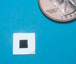
Shining intense, ultrashort laser pulses on the surface of a crystalline silicon wafer drastically changes the optical, material and electronic properties of the wafer. The resulting textured surface is highly absorbing and looks black to the eye. The properties of this 'black silicon' make it useful for a wide range of commercial devices. In particular, we have been able to fabricate highly-sensitive PIN photodetectors using this material. The sensitivity extends to wavelengths of 1600 nm making them particularly useful for applications in communications and remote sensing.
Black silicon: Engineering an intermediate band in silicon for sensing and energy harvesting, at Nanophotonics and Plasmonic Technologies Workshop, Harvard University (Cambridge, MA), Friday, May 7, 2010:
Shining intense, ultrashort laser pulses on the surface of a crystalline silicon wafer drastically changes the optical, material and electronic properties of the wafer. The resulting textured surface is highly absorbing and looks black to the eye. The properties of this 'black silicon' make it useful for a wide range of commercial devices. In particular, we have been able to fabricate highly-sensitive PIN photodetectors using this material. The sensitivity extends to wavelengths of 1600 nm making them particularly useful for applications in communications and remote sensing.
Black silicon, at Harvard Energy Innovation Showcase, Harvard University (Cambridge, MA), Tuesday, November 29, 2011:
Shining intense, ultrashort laser pulses on the surface of a crystalline silicon wafer drastically changes the optical, material and electronic properties of the wafer. The resulting textured surface is highly absorbing and looks black to the eye. The properties of this 'black silicon' make it useful for a wide range of applications including improved solar energy harvesting.
Serendipity and the quest for new materials, at 9th Science and Technology in Society Forum (Kyoto, Japan), Monday, October 8, 2012:
Throughout history, the development of new materials and serendipity have been tightly interwoven. I will illustrate the need for exploration and risk-taking with two anecdotes
Black silicon and the quest for intermediate band semiconductors, at Laser-Based Micro and Nano Processing VIII, Photonics West 2014 (San Francisco, CA), Thursday, February 6, 2014:
Shining intense, ultrashort laser pulses on the surface of a crystalline silicon wafer drastically changes the optical, material and electronic properties of the wafer. The process has two effects: it structures the surface and incorporate dopants into the sample to a concentration highly exceeding the equilibrium solubility limit. This femtosecond laser "hyperdoping technique" enables the fabrication of defect- and bandgap engineered semiconductors, and laser texturing further enhances the optical density through excellent light trapping. Hyperdoped silicon opens the door for novel... Read more about Black silicon and the quest for intermediate band semiconductors
Early stages of femtosecond laser-induced formation of silicon microspikes, at Materials Research Society Fall Meeting (Boston, MA), Monday, December 2, 2002:
Arrays of sharp conical spikes form on crystalline silicon surfaces when irradiated with a train of femtosecond laser pulses in a background of sulfur hexafluoride (SF6); blunter, more irregular microstructures form in vacuum. The tips of the spikes are at the height of the original surface of the wafer, suggesting that the formation process predominantly involves removing material. The spikes are arranged in a quasi-ordered fashion with a characteristic nearest-neighbor separation of a few micrometers; the exact value of this characteristic separation depends on the laser fluence and number... Read more about Early stages of femtosecond laser-induced formation of silicon microspikes
Femtosecond laser-nanostructured substrates for surface enhanced Raman scattering (SERS), at Photonics West 2007 (San Jose, CA), Thursday, January 25, 2007:
We present a new substrate for efficient surface enhanced Raman scattering (SERS). Using a train of focused frequency-doubled femtosecond laser pulses from a regeneratively amplified Ti:Sapphire laser, we fabricate submicron surface structures on a silicon wafer. After irradiating the silicon wafer with 400nm, 100fs laser pulses in a cuvette of water, we observe the formation of an array of spikes, each approximately 500nm tall and 200nm wide. The wafer is scanned across the beam to form an arbitrarily-sized nanostructured area. When covered with a thin film of a noble metal, the structured... Read more about Femtosecond laser-nanostructured substrates for surface enhanced Raman scattering (SERS)
Black silicon, at Huang Kun Forum on Semiconductor Sciences and Technologies, Institute of Semiconductors, Chinese Academy of Sciences (Beijing, China), Tuesday, December 22, 2009:
Shining intense, ultrashort laser pulses on the surface of a crystalline silicon wafer drastically changes the optical, material and electronic properties of the wafer. The resulting textured surface is highly absorbing and looks black to the eye. The properties of this 'black silicon' make it useful for a wide range of commercial devices. In particular, we have been able to fabricate highly-sensitive PIN photodetectors using this material. The sensitivity extends to wavelengths of 1600 nm making them particularly useful for applications in communications, remote sensing, and photovoltaics.
Black silicon: engineering an intermediate band in silicon for optical sensing and photovoltaics, at G1 Faculty Lecture, Harvard University (Cambridge, MA), Monday, November 8, 2010:
Shining intense, ultrashort laser pulses on the surface of a crystalline silicon wafer drastically changes the optical, material and electronic properties of the wafer. The resulting textured surface is highly absorbing and looks black to the eye. The properties of this 'black silicon' make it useful for a wide range of commercial devices. In particular, we have been able to fabricate highly-sensitive PIN photodetectors using this material. The sensitivity extends to wavelengths of 1600 nm making them particularly useful for applications in communications and remote sensing.
Femtosecond laser doping of TiO2 for photocatalysis, at Gordon Research Seminar on Renewable Energy: Solar Fuels (Barga, Italy), Saturday, May 12, 2012:
We present a novel method for femtosecond-laser doping of titanium dioxide (TiO2) for above bandgap absorptance by irradiating titanium metal in the presence of oxygen and dopants. With a bandgap of 3.2 eV for the anatase crystalline phase, TiO2 most strongly absorbs in the UV range (λ < 387 nm). However, doping with metals and nitrogen has been shown to create intermediate states in the bandgap. Using femtosecond laser doping techniques on titanium in a gaseous environment, we produce laser-induced periodic surface structures. Altering the gas composition and pressure does not change the... Read more about Femtosecond laser doping of TiO2 for photocatalysis
Pushing a physics discovery towards commercial impact, at REU Seminar, Harvard University (Cambridge, MA), Wednesday, July 24, 2013:
In 1997 my research group discovered that shining intense, ultrashort laser pulses on the surface of a crystalline silicon wafer drastically changes the optical, material and electronic properties of the wafer. The resulting textured surface is highly absorbing and looks black to the eye, making this 'black silicon' useful for a wide range of commercial devices, from highly-sensitive detectors to improved photovoltaics. Over the following ten years we investigated this material and developed a prototype detector. The prototype gave us the confidence to commercialize black silicon. Together... Read more about Pushing a physics discovery towards commercial impact

Pages