Optical hyperdoping: black silicon

Femtosecond laser-structured silicon: properties and structure, at Gordon Conference on Laser Interactions With Materials (Andover, NH), Tuesday, July 23, 2002:
Silicon surfaces that are microstructured with femtosecond laser pulses in a sulfur hexafluoride environment exhibit several remarkable properties, including near-unity below-band gap optical absorption (C. Wu et al., Appl. Phys. Lett. 78, 1850 (2001)). We report new structural and chemical characterization of this material, including cross-sectional TEM images of the microstructures. Our results indicate that the below-band gap absorption most likely comes from a surface layer of polycrystalline silicon roughly 1 micrometer thick, which includes nanopores, nanocrystals, and a high... Read more about Femtosecond laser-structured silicon: properties and structure
Femtosecond laser-assisted microstructuring of silicon surfaces for novel detector, sensing, and display technologies, at 41st Annual Technical Meeting of the Society of Engineering Science, University of Nebraska, Lincoln (Lincoln, NE), Monday, October 11, 2004:
Irridiating silicon surfaces with trains of ultrashort laser pulses in the presence of a sulfur containing gas drastically changes the structure and properties of silicon. The normally smooth and highly reflective surface develops a forest of sharp microscopic spikes. The microstructured surface is highly absorbing even at wavelengths beyond the bandgap of silicon and has many interesting novel applications.
Femtosecond laser doping of silicon: Electronic structure, at CLEO 2008 (San Jose, CA), Thursday, May 8, 2008:
Shining intense, ultrashort laser pulses on the surface of a crystalline silicon wafer drastically changes the optical, material and electronic properties of the wafer. The resulting textured surface is highly absorbing and looks black to the eye. The properties of this 'black silicon' make it useful for a wide range of commercial devices. In particular, we have been able to fabricate highly-sensitive PIN photodetectors using this material. The sensitivity extends to wavelengths of 1600 nm making them particularly useful for applications in communications and remote sensing. We have performed... Read more about Femtosecond laser doping of silicon: Electronic structure
Black silicon, at University of Queensland (Brisbane, Australia), Friday, January 15, 2010:
Shining intense, ultrashort laser pulses on the surface of a crystalline silicon wafer drastically changes the optical, material and electronic properties of the wafer. The resulting textured surface is highly absorbing and looks black to the eye. The properties of this 'black silicon' make it useful for a wide range of commercial devices. In particular, we have been able to fabricate highly-sensitive PIN photodetectors using this material. The sensitivity extends to wavelengths of 1600 nm making them particularly useful for applications in communications and remote sensing.
Transforming the optical properties of silicon using femtosecond laser pulses, at Horizons of Nanophotonics and Nanoelectronics, a Keio-Harvard Workshop, Harvard University (Cambridge, MA), Monday, December 20, 2010:
We developed a technique, optical hyperdoping (OHD), for doping semiconductors to unusually high levels and endowing them with remarkable optoelectronic properties. By irradiating Si with a train of femtosecond laser pulses in the presence of chalcogen (column VI) compounds, a 300-nm thin layer of Si is doped to previously unreported, non-equilibrium levels (about 1%). When the dopant is chosen from the heavy chalcogens (sulfur, selenium, tellurium), the doped silicon exhibits remarkable optoelectronic properties: near-unity absorptance from the ultraviolet ( λ < 250 nm) to the near-... Read more about Transforming the optical properties of silicon using femtosecond laser pulses
Femtosecond laser doping of TiO2 for photocatalysis, at Gordon Research Conference on Renewable Energy: Solar Fuels (Barga, Italy), Wednesday, May 16, 2012:
We present a novel method for femtosecond-laser doping of titanium dioxide (TiO2) for above bandgap absorptance by irradiating titanium metal in the presence of oxygen and dopants. With a bandgap of 3.2 eV for the anatase crystalline phase, TiO2 most strongly absorbs in the UV range (λ < 387 nm). However, doping with metals and nitrogen has been shown to create intermediate states in the bandgap. Using femtosecond laser doping techniques on titanium in a gaseous environment, we produce laser-induced periodic surface structures. Altering the gas composition and pressure does not change the... Read more about Femtosecond laser doping of TiO2 for photocatalysis
Towards increased efficiency in solar energy harvesting via intermediate states, at SPIE Laser Material Processing for Solar Energy Devices II (San Diego, CA), Wednesday, August 28, 2013:
Shining intense, ultrashort laser pulses on the surface of a crystalline silicon wafer drastically changes the optical, material and electronic properties of the wafer. The process has two effects: it structures the surface and incorporate dopants into the sample to a concentration highly exceeding the equilibrium solubility limit. This femtosecond laser "hyperdoping technique" enables the fabrication of defect- and bandgap engineered semiconductors, and laser texturing further enhances the optical density through excellent light trapping. Hyperdoped silicon opens the door for novel... Read more about Towards increased efficiency in solar energy harvesting via intermediate states
Femtosecond-Laser Hyperdoping and Texturing of Silicon for Advanced Non-equilibrium Materials, at 2014 AFOSR Ultrashort Pulse Laser-Matter Interactions Program Review (Arlington, VA), Friday, May 30, 2014:
Shining intense, ultrashort laser pulses on the surface of a crystalline silicon wafer drastically changes the optical, material and electronic properties of the wafer. The process has two effects: it structures the surface and incorporate dopants into the sample to a concentration highly exceeding the equilibrium solubility limit. This femtosecond laser "hyperdoping technique" enables the fabrication of defect- and bandgap engineered semiconductors, and laser texturing further enhances the optical density through excellent light trapping. Hyperdoped silicon opens the door for novel... Read more about Femtosecond-Laser Hyperdoping and Texturing of Silicon for Advanced Non-equilibrium Materials
Black silicon: hot properties and many open questions, at Atomic and molecular physics at surfaces, ITAMP (Cambridge, MA), Thursday, June 14, 2001:
A serendipitous discovery in our lab produced a novel form of microstructured silicon ("black silicon") that has many surprising properties: near unity absorption, even below the bandgap; production of photoelectrons in the visible and infrared; visible luminescence; and a strong field emission current. We are beginning to shed light on what might cause some of the material's remarkable properties. Much additional experimental and theoretical work is required to understand the surface physics and chemistry that leads to the formation of black silicon.
Femtosecond laser ablation of silicon: nanoparticles, doping and photovoltaics, at Harvard University (Thesis Defense) (Cambridge, MA), Friday, April 27, 2007:

In this thesis, we investigate the irradiation of silicon in a background gas of near atmospheric pressure with intense femtosecond laser pulses at energy densities exceeding the threshold for ablation (the macroscopic removal of material). We study the resulting structure and properties of the material ejected in the ablation plume as well as the laser irradiated surface itself.

The material collected from the ablation plume is a mixture of single crystal silicon nanoparticles and a highly porous network of amorphous silicon. The crystalline nanoparticles form by nucleation...

Read more about Femtosecond laser ablation of silicon: nanoparticles, doping and photovoltaics
Black silicon, at Technical University of Denmark (Copenhagen, Denmark), Tuesday, June 16, 2009:
Shining intense, ultrashort laser pulses on the surface of a crystalline silicon wafer drastically changes the optical, material and electronic properties of the wafer. The resulting textured surface is highly absorbing and looks black to the eye. The properties of this 'black silicon' make it useful for a wide range of commercial devices. In particular, we have been able to fabricate highly-sensitive PIN photodetectors using this material. The sensitivity extends to wavelengths of 1600 nm making them particularly useful for applications in communications and remote sensing.
Infrared absorption limits of femtosecond laser doped silicon – effect of dopant types and thermal treatments, at Black Silicon Symposium (Albany, NY), Friday, August 20, 2010
Silicon doped with non-equilibrium concentrations of chalcogen exhibits strong sub-bandgap photon absorption. In this work, we investigate mid-infrared absorption of femtosecond laser doped silicon. Fourier transform infrared spectroscopy could shed light on energy levels of dopant states or bands. We study samples doped with sulfur, selenium and tellurium. In addition, we also investigate the effect of annealing temperature. Preliminary results suggest that near-unity absorption of sulfur doped silicon extends to mid-infrared. However, absorption decreases for photons with energy less than... Read more about Infrared absorption limits of femtosecond laser doped silicon – effect of dopant types and thermal treatments
Femtosecond-laser hyperdoping: controlling sulfur concentrations in silicon for band gap engineering, at APS March meeting (Boston, MA), Tuesday, February 28, 2012:
Doping silicon to concentrations above the metal-insulator transition threshold yields a novel material that has potential for photovoltaic applications. By focusing femtosecond laser pulses on the surface of a silicon wafer in a sulfur hexafluoride (SF6) environment, silicon is doped with 1% atomic sulfur. This material exhibits near-unity, broadband absorption from the visible to the near infrared (< 0.5 eV, deep below the silicon bandgap), and metallic-like conduction. These unusual optical and electronic properties suggest the formation of an intermediate band. We report on the... Read more about Femtosecond-laser hyperdoping: controlling sulfur concentrations in silicon for band gap engineering
Black silicon and the quest for intermediate band semiconductors, at Zhejiang University (Hangzhou, China), Thursday, December 13, 2012:
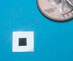
Shining intense, ultrashort laser pulses on the surface of a crystalline silicon wafer drastically changes the optical, material and electronic properties of the wafer. The resulting textured surface is highly absorbing and looks black to the eye. The properties of this 'black silicon' make it useful for a wide range of commercial devices. In particular, we have been able to fabricate highly-sensitive PIN photodetectors using this material. The sensitivity extends to wavelengths of 1600 nm making them particularly useful for applications in communications and remote sensing.

Pages