Optical hyperdoping: black silicon

Serendipity, science, and engineering, at Sophomore forum, Harvard University (Cambridge, MA), Monday, February 7, 2011:
Shining intense, ultrashort laser pulses on the surface of a crystalline silicon wafer drastically changes the optical, material and electronic properties of the wafer. The resulting textured surface is highly absorbing and looks black to the eye. The properties of this 'black silicon' make it useful for a wide range of commercial devices. In particular, we have been able to fabricate highly-sensitive PIN photodetectors using this material. The sensitivity extends to wavelengths of 1600 nm making them particularly useful for applications in communications and remote sensing.
Femtosecond Laser Nanostructuring of Semiconductors and Metals, at 13th International Symposium on Laser Precision Microfabrication (LPM), The Catholic University of America (Washington, DC), Thursday, June 14, 2012:
We have developed a unique technique to change the optoelectronic properties of many materials through hyperdoping and texturing [1]. By irradiating materials, such as silicon and titanium dioxide, with a train of amplified femtosecond (fs) laser pulses in the presence of a wide variety of dopant precursors, we can introduce dopants above the solubility limit while producing surface structures that have excellent anti-reflection and light-trapping properties.

Femtosecond-laser texturing originates from the formation of laser induced period surface structures (LIPSS) and consists of semi...

Read more about Femtosecond Laser Nanostructuring of Semiconductors and Metals
Pushing a physics discovery towards commercial impact, at REU Seminar, Harvard University (Cambridge, MA), Wednesday, July 16, 2014:
In 1997 my research group discovered that shining intense, ultrashort laser pulses on the surface of a crystalline silicon wafer drastically changes the optical, material and electronic properties of the wafer. The resulting textured surface is highly absorbing and looks black to the eye, making this 'black silicon' useful for a wide range of commercial devices, from highly-sensitive detectors to improved photovoltaics. Over the following ten years we investigated this material and developed a prototype detector. The prototype gave us the confidence to commercialize black silicon. Together... Read more about Pushing a physics discovery towards commercial impact
Black silicon: From accidental discovery to company, at the Society for Creativity and Innovation, Harvard University (Cambridge, MA), Monday, November 19, 2007:
Shining intense, ultrashort laser pulses on the surface of a crystalline silicon wafer drastically changes the optical, material and electronic properties of the wafer. The resulting textured surface is highly absorbing and looks black to the eye. The properties of this 'black silicon' make it useful for a wide range of commercial devices. In particular, we have been able to fabricate highly-sensitive PIN photodetectors using this material. The sensitivity extends to wavelengths of 1600 nm making them particularly useful for applications in communications and remote sensing.
Optical Hyperdoping: Silicon sees the infrared light, at Applied Physics Colloquium, Harvard University (Cambridge, MA), Friday, October 9, 2009:
Shining intense, ultrashort laser pulses on the surface of a crystalline silicon wafer drastically changes the optical, material and electronic properties of the wafer. The resulting textured surface is highly absorbing and looks black to the eye. The properties of this 'black silicon' make it useful for a wide range of commercial devices. In particular, we have been able to fabricate highly-sensitive PIN photodetectors using this material. The sensitivity extends to wavelengths of 1600 nm making them particularly useful for applications in communications and remote sensing.
Black silicon: silicon sees the light, at Graduate Consortium on Energy and Environment Seminar, Harvard University (Cambridge, MA), Friday, September 17, 2010:
Shining intense, ultrashort laser pulses on the surface of a crystalline silicon wafer drastically changes the optical, material and electronic properties of the wafer. The resulting textured surface is highly absorbing and looks black to the eye. The properties of this 'black silicon' make it useful for a wide range of commercial devices. In particular, we have been able to fabricate highly-sensitive PIN photodetectors using this material. The sensitivity extends to wavelengths of 1600 nm making them particularly useful for applications in communications and remote sensing.
Hyperdoped and microstructured silicon for solar energy harvesting, at PIERS 2012 (Kuala Lumpur, Malaysia), Wednesday, March 28, 2012:
We have developed a unique technique to significantly change the optoelectronic properties of silicon through hyperdoping and texturing. By irradiating silicon with a train of amplified femtosecond laser pulses in the presence of a wide variety of dopant precursors, we can hyperdope silicon to > 1 at.% in a 300-nm thin layer. In addition, laser-induced semi-periodic surface textures have excellent anti-reflection and light-trapping properties. The technique is robust: it is effective on both crystalline and amorphous silicon and for both thin films and thick substrates. When the dopant is... Read more about Hyperdoped and microstructured silicon for solar energy harvesting
The photovoltaic potential of femtosecond laser textured amorphous silicon, at Photonics West (San Francisco, CA), Thursday, February 7, 2013:
Femtosecond laser texturing of silicon yields nanometer scale surface roughness that reduces reflection and enhances light absorption. In this work, we study the potential of using this technique to improve efficiencies of amorphous silicon-based solar cells by laser texturing thin amorphous silicon films. We use Ti:Sapphire femtosecond laser systems to texture amorphous silicon in either hydrogen or sulfur hexafluoride ambient gases and we also study the effect of laser texturing the substrate before depositing amorphous silicon. We adjust the thin-film thickness and laser fabrication... Read more about The photovoltaic potential of femtosecond laser textured amorphous silicon
Laser-processing of semiconductors and (some) applications , at HUCE Lunch Seminar, Harvard University (Cambridge, MA), Friday, January 31, 2014:
Shining intense, ultrashort laser pulses on the surface of a crystalline silicon wafer drastically changes the optical, material and electronic properties of the wafer. The resulting textured surface is highly absorbing and looks black to the eye. The properties of this 'black silicon' make it useful for a wide range of commercial devices. In particular, we have been able to fabricate highly-sensitive PIN photodetectors using this material. The sensitivity extends to wavelengths of 1600 nm making them particularly useful for applications in communications and remote sensing.
Laser doping and texturing of silicon for advanced optoelectronic devices, at Tsing Hua University (Hsinchu, Taiwan), Wednesday, June 29, 2016:
Irradiating a semiconductor sample with intense laser pulses in the presence of dopants drastically changes the optical, material and electronic properties of the sample. The properties of these processed semiconductors make them useful for photodetectors and, potentially, intermediate band solar cells. This talk discusses the processes that lead to doping and surface texturing, which both increase the optical absorption of the material. We will discuss the properties of the resulting material including the formation of an intermediate band. We have developed laser-processed silicon... Read more about Laser doping and texturing of silicon for advanced optoelectronic devices
Femtosecond laser-assisted microstructuring of silicon for novel detector, sensing, and display technologies, at IEEE/LEOS 2002 Conference on Electro-Optic Sensors and Systems (Glasgow, Scotland), Monday, November 11, 2002:
Arrays of sharp, conical microstructures are obtained by texturing the surface of a silicon wafer using femtosecond laser-assisted chemical etching. The one step, maskless texturing process drastically changes the optical, material and electronic properties of the original silicon wafer. These properties make the textured silicon viable for use in a wide range of commercial devices. First, near-unity absorption of light, from visible to infrared wavelengths, offer opportunities for use in optically active devices such as solar cells and detectors. Significant enhancement of below-band-gap... Read more about Femtosecond laser-assisted microstructuring of silicon for novel detector, sensing, and display technologies
Femtosecond-laser microstructuring of silicon for photovoltaic devices, at Photonics West 2006 (San Jose, CA), Tuesday, January 24, 2006:
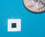
Photovoltaics research has recently focused on photovoltaic materials made by cheaper processes with minimal waste such as thin-films grown by chemical vapor deposition. Because silicon is the most common semiconductor material and the second most abundant element in the earth, silicon-based thin films are an excellent choice for photovoltaics. The drawback to crystalline silicon thin films is low absorption due to silicon’s indirect band gap. Thicker films increase processing costs and sacrifice efficiency due to defects inherent in the thin-films.

We report the creation of a thin,...

Read more about Femtosecond-laser microstructuring of silicon for photovoltaic devices

Pages